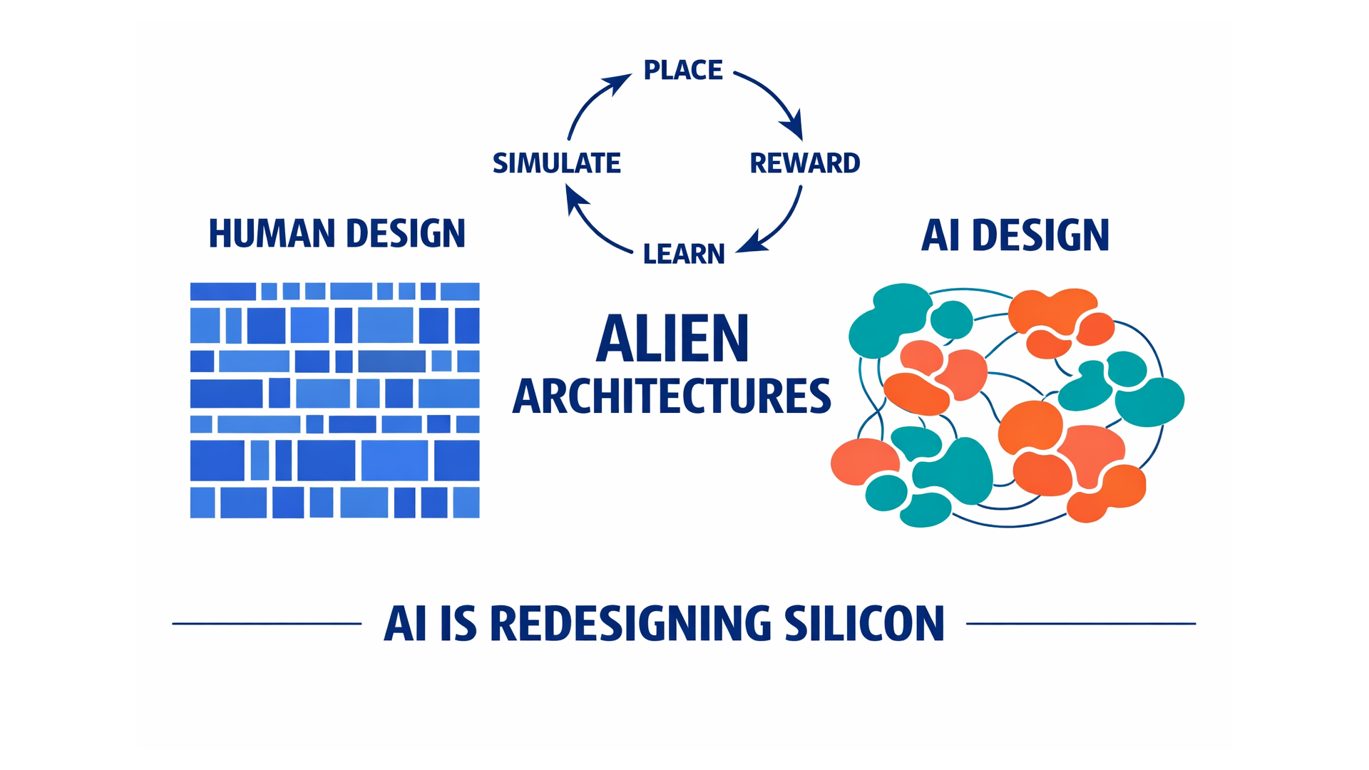
A modern high-end processor contains more transistors than there are stars in the Milky Way. And the number of ways to arrange those transistors on a chip exceeds the number of atoms in the observable universe. For fifty years, we solved this problem the same way: human engineers using rules of thumb from the 1980s. That era is over.
Moore's Law — the engine that powered the entire digital economy — is stalling. Not because we can't make transistors smaller, but because shrinking them no longer delivers the performance gains it used to. The cost per transistor at cutting-edge nodes is now rising, not falling. And the design complexity has blown past what human cognition can handle. I've spent the last two years studying what comes next, and I'm now convinced the answer is counterintuitive: the chips of the future will be designed by AI agents playing a game — and the layouts they produce will look like nothing a human engineer would ever draw.
Why Did Moore's Law Actually Die?
Most people think Moore's Law is about making transistors smaller. It's really an economic observation: smaller transistors meant cheaper transistors, which meant you could pack more onto a chip for less money. That virtuous cycle drove five decades of computing progress.
Two things broke the cycle.
First, power density stopped cooperating. A companion principle called Dennard Scaling used to guarantee that as transistors shrank, they'd use proportionally less power. That collapsed in the mid-2000s. Today, chips run so hot that a significant percentage of transistors must stay powered off at any given time just to prevent thermal damage — a phenomenon the industry calls "Dark Silicon."
Second, and this is the part most people miss: the bottleneck moved from the transistor to the wire. In today's nanometer-scale chips, a signal can zip through a logic gate in picoseconds. But traveling across the chip through the maze of microscopic copper wires? That takes nanoseconds — orders of magnitude slower. The physical arrangement of components on the chip now matters more than the transistors themselves.
The fastest transistor in the world is useless if the wire connecting it to the next one is too long.
This means chip floorplanning — deciding where to physically place billions of components — has become the single most important factor in whether a chip is fast or slow, efficient or power-hungry. And that's exactly where human engineers have hit a wall.
Why Can't Human Engineers Keep Up?
Think of chip design like arranging furniture in a house — except the house has a billion rooms, every piece of furniture is connected to dozens of others by wires that must be as short as possible, and you're simultaneously optimizing for airflow, electrical interference, manufacturing constraints, and cost. Oh, and if you get it wrong, you've wasted $500 million on a fabrication run.
Human engineers manage this by breaking the chip into smaller blocks and optimizing each one separately. It's practical, but it sacrifices the big picture. Fixing a congestion problem in one block might create a timing disaster in the block next door, and no human can mentally simulate those ripple effects across an entire system.
The standard algorithmic tool for this job — Simulated Annealing — dates back to the 1980s. It works by randomly shuffling components and gradually "cooling" toward a solution. Two problems make it inadequate for modern chips. It's memoryless: every run starts from scratch, learning nothing from previous designs. And it gets trapped in "good enough" solutions because it can't perceive better options hidden in the vast landscape of possibilities.
The result? Teams of expert engineers spend weeks or months manually tweaking layouts, moving components by hand to fix problems that the algorithms missed. This human bottleneck is why advanced chip development now costs billions and takes years.
What Happens When Chip Design Becomes a Game?
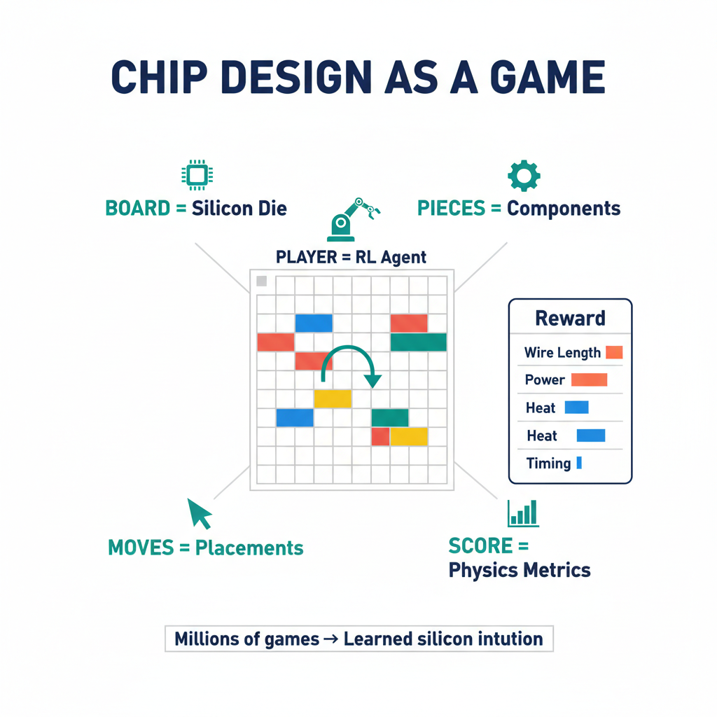
This is where my thinking shifted. What if we stopped treating chip layout as an optimization equation and started treating it as a game — like Chess or Go?
The silicon die is the board. The components are the pieces. Each placement is a move. And the score is a composite of real physics: wire length, power consumption, heat distribution, timing. An AI agent plays this game millions of times, learning not from rules a human programmed, but from the physics-based rewards it receives.
This is Deep Reinforcement Learning applied to silicon — the same family of techniques that produced AlphaGo and trained ChatGPT. We explored the full technical framework in our interactive analysis, but the core insight is simple: an RL agent develops something like intuition. It learns that placing memory controllers near I/O interfaces reduces latency. It learns that certain clustered arrangements of arithmetic units reduce congestion. Not because anyone told it — because it was rewarded for discovering these patterns on its own.
Reinforcement learning doesn't follow rules of thumb. It discovers the rules that the thumbs missed.
And then something strange happens. The first time I saw an AI-generated chip layout, my reaction was: this looks broken. Components scattered in irregular clusters. Logic clouds in amorphous blobs. No neat rows, no symmetry, no recognizable structure. Human engineers have a name for the traditional approach — "Manhattan" layout, because it resembles a city grid. The AI's output looked more like a Jackson Pollock painting.
But when we ran the physics simulations, the "messy" layouts consistently outperformed the clean human designs. Shorter wire lengths. Better thermal distribution. Fewer timing violations.
The chaos was actually a higher form of order — one optimized for electron flow rather than human comprehension. The AI had discovered that the shortest path for a signal is rarely a straight line along a grid. It's an intricate weave through available space that no human would intuit but that physics rewards.
I started calling these "alien architectures" — layouts that look wrong to human eyes but are verified by physics to run faster and cooler. That moment changed how I think about the entire field.
Who's Already Shipping AI-Designed Silicon?
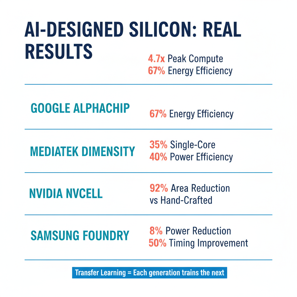
Google's AlphaChip, first published in Nature in 2021, was the moment this went from theoretical to undeniable. Their team trained a reinforcement learning agent to design layouts for Google's Tensor Processing Units — the custom chips that power everything from Google Search to Gemini.
The technical innovation that made it work: instead of treating the chip's component list as text, AlphaChip perceives it as a graph. A specialized neural network called an Edge-GNN (Graph Neural Network) creates a map of how every component connects to every other component, capturing the topology — which parts need to be close together, which create congestion when clustered.
Two networks work in tandem. A Policy Network predicts the best next placement. A Value Network estimates how good the final chip will be from any partial state. Together, they guide the agent through the astronomical search space with something resembling strategic foresight.
But the real superpower is transfer learning. Google pre-trained the agent on a diverse set of chip designs — memory controllers, processor cores, interface blocks, open-source RISC-V (an open-source processor architecture) designs. When presented with a brand-new chip block it had never seen, the agent didn't start from zero. It started with generalized intuition about silicon physics, then refined it. What took human teams weeks, the agent accomplished in hours.
The results on Google's latest Trillium TPUs: a 4.7x increase in peak compute performance and a 67% improvement in energy efficiency compared to the previous generation, with AlphaChip designing an increasing proportion of the blocks.
And this isn't just a Google trick. MediaTek applied AlphaChip principles to their Dimensity flagship chips — the processors inside millions of Android smartphones. The Dimensity 9400 delivered 35% better single-core performance, 40% better power efficiency, and doubled AI processing capability while using 33% less power. These gains come from process improvements and architectural changes too, but MediaTek explicitly credited RL-driven floorplanning for enabling the layouts that made the numbers possible — particularly in optimizing the placement of cache and memory controller hierarchies.
Meanwhile, NVIDIA attacked the problem from the opposite end of the scale. Their NVCell framework uses reinforcement learning to optimize the internal layout of individual logic gates — the atomic building blocks of every digital chip. NVCell generates layouts that are 92% smaller or equal in area to hand-crafted designs by expert engineers, with zero human intervention. When you shrink the building blocks themselves, every chip built from them gets smaller and more efficient. The advantage multiplies.
Samsung Foundry reported using similar AI-driven flows to reduce power by 8% on critical blocks and improve timing by over 50% — in weeks rather than months.
For the full technical methodology behind these approaches and our comparative analysis, see our detailed research.
Why Does "AI for Chip Design" Usually Mean the Wrong Thing?
I need to draw a sharp line here, because "AI for EDA (Electronic Design Automation)" has become a marketing buzzword that covers wildly different things.
Most offerings in the market today are what I'd call parameter tuners. Synopsys DSO.ai, for example, is excellent at running the same traditional placement tool hundreds of times with different settings and finding the best configuration. Cadence Cerebrus automates the flow between design steps. Both are valuable productivity tools.
But neither changes the underlying physics of the design. They're optimizing the knobs on an old engine. What reinforcement learning does is replace the engine entirely. The AI agent is the placer — it makes millions of direct placement decisions based on learned physics, not scripted commands.
Tuning the parameters of a 1980s algorithm is not the same as replacing the algorithm with learned intelligence.
The practical difference shows up in what's possible. Parameter tuning finds the best version of a conventional layout. Deep RL discovers layouts that conventional tools literally cannot produce — the alien architectures that outperform human intuition.
Every veteran engineer I've talked to has the same reaction to alien layouts: "Why did it put that block there? How do I know it's not a hallucination?"
This is the right question, and it's the one that separates serious AI-for-silicon work from demos. The answer isn't "trust the AI." The answer is making the AI's reasoning visible.
We build what I think of as reward trajectory maps — visualizations that show which constraints drove each placement decision. Was it congestion avoidance? Thermal management? A timing-critical path? When an engineer can see that the AI placed a clock divider in an unexpected location because it detected a congestion hotspot that wasn't visible in the traditional view, trust follows naturally.
The other objection I hear: "Training RL agents requires massive GPU compute. Isn't that prohibitively expensive?" It's a fair concern, but it misframes the economics. The traditional approach burns millions in engineering salaries and months of calendar time on every design iteration. RL training is a one-time capital investment, and transfer learning means you don't retrain from scratch for each new chip. You fine-tune. The marginal cost of generating a new design drops dramatically after the initial investment.
What This Means If You're Building Silicon
Moore's Law gave the semiconductor industry a free ride for fifty years: shrink the transistors, get automatic speedups. That ride is over. But the demand for compute — driven by the very AI we're discussing — is accelerating exponentially.
The gap between what physics gives us for free and what the market demands can only be closed by arranging transistors smarter, not smaller. I've started calling this Complexity Scaling — extracting performance not from better manufacturing, but from better design intelligence.
Three things follow from this:
Your legacy designs are training data. Every chip your team has taped out contains embedded knowledge about what works and what doesn't. Cleaned and normalized, that history becomes the foundation for an RL agent that embodies your organization's collective design intuition. Most companies treat old design files as archives. They're actually competitive assets.
The team structure changes too — and more radically than most leaders expect. The elite design team of the near future isn't fifty engineers doing manual layout. It's five engineers guiding a fleet of RL agents, reviewing alien architectures, and making strategic decisions about which constraints matter most. The human role shifts from placement to judgment.
And the window for catching up is closing fast. Google, MediaTek, NVIDIA, and Samsung are already shipping silicon designed this way. Every generation of AI-designed chips produces training data that makes the next generation better — a compounding advantage that late adopters can't shortcut.
I don't know exactly what chips will look like in ten years. But I'm increasingly certain they won't look like anything a human would draw. The layouts will be alien. The physics will be undeniable. And the companies that embraced the strangeness early will be the ones still competing.
If you're navigating this transition — whether you're a design team lead, a VP of engineering, or a semiconductor strategist trying to figure out what's real versus what's hype — I'd genuinely like to hear how you're thinking about it.