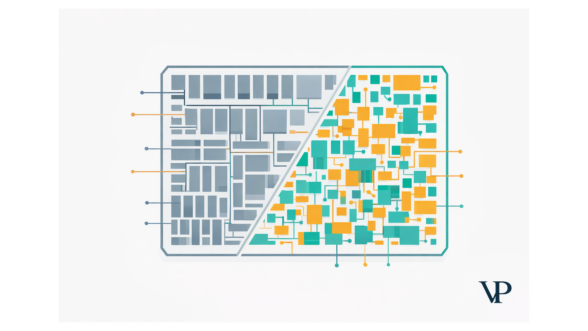
A modern high-end processor contains more transistors than there are stars in the Milky Way. Arranging those billions of components to minimize heat, maximize speed, and reduce power consumption involves a design space larger than the number of atoms in the observable universe. And the engineers responsible for this work? They've been relying on optimization algorithms invented in the 1980s.
The semiconductor industry has a problem that no amount of human ingenuity can solve alone. Moore's Law — the five-decade engine of computing progress — is stalling. Transistors can't shrink much further without bumping into the laws of quantum physics. The cost per transistor at cutting-edge manufacturing nodes is rising, not falling. And the performance gains from each new generation are diminishing.
Our team has been studying how reinforcement learning — the same family of AI that mastered Chess and Go — is being applied to chip design. What we found is a paradigm shift already underway at Google, NVIDIA, and MediaTek. The results are startling: AI agents are producing chip layouts that look like nothing a human would design, yet consistently outperform human-crafted alternatives when tested against real physics. We published our full analysis of this transformation to map where the industry is heading.
The Real Bottleneck Isn't the Transistor — It's the Wire
Most people assume chip performance is about making transistors faster. That stopped being true years ago.
In today's nanometer-scale chips, a signal can pass through a logic gate in trillionths of a second. But traveling across the chip through microscopic copper wires? That takes orders of magnitude longer. The resistance and capacitance of those tiny interconnects now dominate both speed and power consumption.
This means the physical arrangement of components on the chip — what engineers call "floorplanning" — has become the single most important factor in performance. A brilliant circuit design with a poor layout will always lose to an average circuit with a great layout.
The bottleneck in modern chips isn't the speed of the transistor. It's the length of the wire.
Human engineers handle this by organizing components into neat, grid-like structures — think city blocks in Manhattan. These layouts are easy for people to reason about, debug, and iterate on. But "easy to understand" and "physically optimal" are not the same thing. The shortest path for an electrical signal is rarely a straight line along a grid.
Why 1980s Algorithms Can't Design 2025 Chips
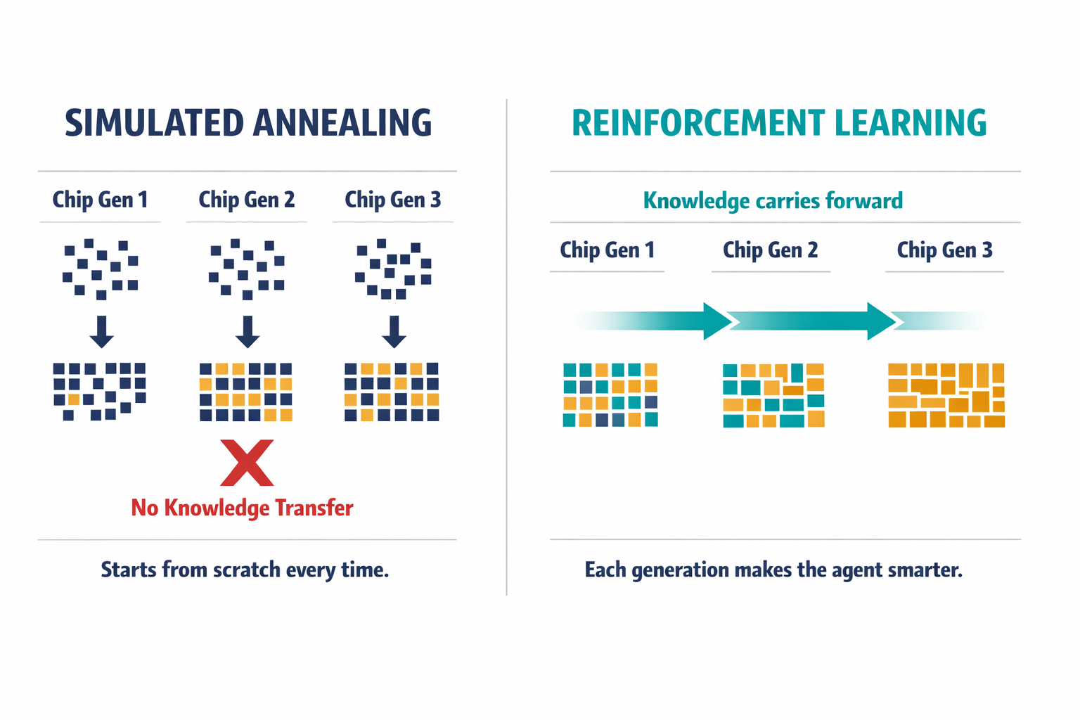
The standard tool for chip floorplanning is an algorithm called Simulated Annealing. It works by randomly rearranging components, evaluating the result, and gradually "cooling" toward a solution — like shaking a box of parts and hoping they settle into a good configuration.
Two problems make this approach increasingly inadequate.
First, it's memoryless. Every time you run it, it starts from scratch. It learns nothing from previous runs, and nothing from previous chip generations. A company that has designed dozens of processors over a decade gets zero accumulated wisdom from the algorithm.
Second, it gets stuck. The optimization landscape for a modern chip is so complex — with billions of possible arrangements and thousands of competing constraints — that Simulated Annealing routinely settles for "good enough" solutions. It can't perceive that a radically different arrangement, one that looks worse in the short term, might unlock a globally superior design.
The result is that physical design remains brutally labor-intensive. Teams of expert engineers spend weeks or months manually adjusting layouts, moving memory blocks by hand to fix timing violations that the automated tools missed. This human-in-the-loop bottleneck is a primary driver of both the cost and the timeline for bringing new chips to market.
Treating Chip Design Like a Game of Go
The breakthrough insight — pioneered by Google's AlphaChip project and now spreading across the industry — is deceptively simple: stop treating chip layout as a math problem to be solved, and start treating it as a game to be played.
Think of it this way. The silicon die is the board. The components — memory blocks, logic clusters, I/O interfaces — are the pieces. Each placement decision is a move. And the score is determined by the physical qualities of the final layout: total wire length, power consumption, heat distribution, and whether signals arrive on time.
Reinforcement learning (RL) agents learn by playing this game millions of times. They place a component, observe the consequences, receive a score, and adjust their strategy. Over millions of iterations, they develop something that resembles intuition — not programmed rules, but learned patterns about what makes silicon work well.
An RL agent doesn't follow rules about where to place a memory controller. It discovers those rules by being rewarded when the chip runs faster.
The technical foundation involves representing the chip's circuit as a graph — a web of nodes (components) and edges (wires) — and using a specialized neural network called a Graph Neural Network to understand the topology. The agent learns that certain components are heavily interconnected and should be placed to minimize the wire between them, but it also learns subtler patterns: that placing a routing-heavy block in the center of the die causes congestion three steps later.
"Alien" Layouts That Outperform Human Designs
The most visually striking result of this approach is what researchers have called "alien layouts."
When a human engineer designs a floorplan, it looks organized. Memory blocks line up in columns. Logic regions form tidy rectangles. Everything has a visual logic that another engineer can read and understand.
AI-generated layouts look like controlled chaos. Macros are scattered in irregular clusters. Logic regions appear amorphous. To a trained engineer's eye, it looks wrong.
But when these layouts are simulated against real physics — measuring actual wire length, signal timing, power draw, and heat distribution — they consistently beat the human versions. The apparent disorder is actually a higher form of order, one optimized for electron flow rather than human comprehension.
The "chaos" in AI chip layouts is a hyper-optimization that no human could achieve — because no human can mentally simulate the ripple effects of billions of placement decisions.
This is the core tension the industry is grappling with. The best chip designs are becoming ones that human engineers can't fully explain. They can verify them — the physics simulations confirm they work — but the reasoning behind specific placement decisions is embedded in neural network weights, not in a logic trail a person can follow.
Google's AlphaChip: From Research Paper to Production Silicon
Google's AlphaChip, first published in Nature in 2021, was the proof that this approach works at commercial scale. The system was used to design successive generations of Google's Tensor Processing Units (TPUs) — the custom AI chips that power Google Search, Gmail, and YouTube.
The critical innovation wasn't just the RL agent itself. It was transfer learning — the ability to carry knowledge from one chip design to the next. Google pre-trained the agent on a diverse set of chip blocks: memory controllers, processor cores, I/O interfaces, and open-source RISC-V designs. By practicing on varied layouts, the agent developed general principles of floorplanning.
When presented with a new, unseen chip block, the agent didn't start from zero. It started with pre-trained intuition and converged on a high-quality layout in hours, compared to the weeks a human team would require. Each new chip generation made the agent smarter, creating a compounding advantage that no static algorithm can match.
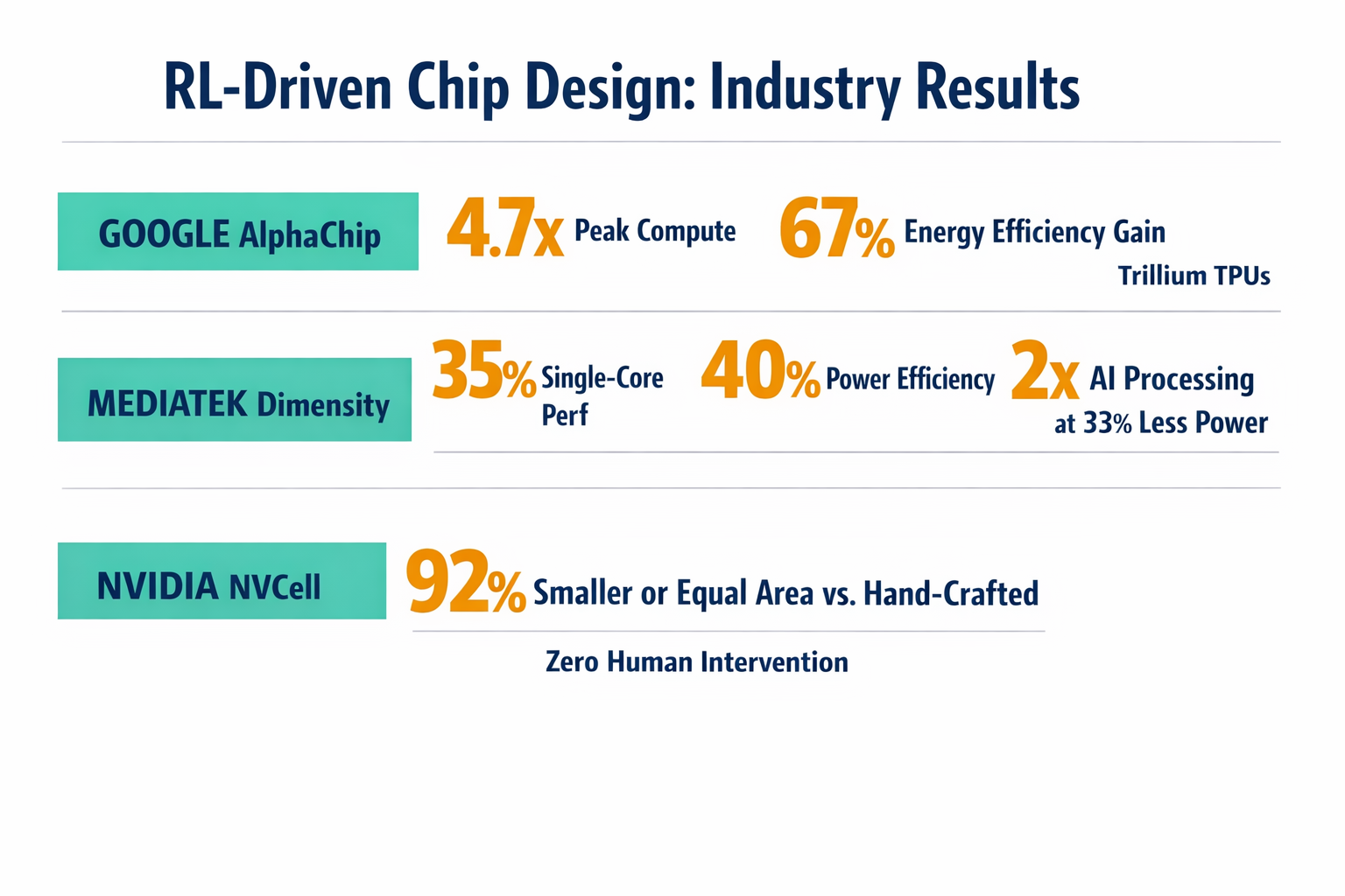
The numbers from Google's latest Trillium TPUs tell the story: 4.7x increase in peak compute performance and 67% improvement in energy efficiency compared to the previous generation, with AlphaChip designing a growing proportion of the chip's blocks.
MediaTek and NVIDIA: Proof This Isn't Just a Google Trick
If AlphaChip only worked inside Google, it could be dismissed as a hyperscaler advantage — a company with effectively unlimited compute and a unified design history. The real validation came when merchant chipmakers adopted similar approaches.
MediaTek, which designs the processors in hundreds of millions of Android smartphones, applied RL-based floorplanning to its flagship Dimensity SoCs. The results across the Dimensity 9400 generation included 35% single-core performance gains, 40% power efficiency improvements, and double the AI processing capability at 33% less power. While these numbers reflect multiple factors — new manufacturing processes, architectural changes — MediaTek executives specifically credited RL-driven placement for enabling the floorplans that delivered the power efficiency gains, particularly in optimizing L3 cache and memory controller placement.
Meanwhile, NVIDIA attacked the problem from the opposite end of the scale. Their NVCell framework uses RL to optimize the layout of standard cells — the tiny building blocks like individual logic gates that number in the millions on a chip. NVCell generates layouts that are 92% smaller or equal in area compared to hand-crafted designs by expert engineers, with zero human intervention. Because standard cells are reused across every chip in a product family, shrinking them creates a multiplicative efficiency gain.
Samsung Foundry has reported similar results: 8% power reduction on critical blocks and timing improvements that compressed months of work into weeks. For the detailed technical methodology behind these advances, our deep-dive research covers the full RL architecture, reward function design, and comparative analysis.
What About the "Black Box" Problem?
The obvious objection: if engineers can't explain why the AI placed a clock divider in an unexpected location, how do they know it isn't a mistake?
This is a legitimate concern, and it's the primary cultural barrier to adoption. A veteran engineer looking at an alien layout has every right to ask whether the AI is hallucinating — producing something that looks optimized but will fail under conditions the training didn't cover.
The answer comes in two parts. First, every AI-generated layout is verified against the same physics simulations that validate human designs. The chip either meets timing, power, and thermal specifications or it doesn't. The verification is deterministic — no ambiguity.
Second, the industry is developing what we'd call explainability dashboards for chip design AI. These tools visualize the agent's decision-making process — showing sensitivity maps that reveal which constraints (congestion, timing, thermal hotspots) drove specific placement decisions. The alien placement turns out not to be random; it's a calculated response to a congestion problem that the human engineer hadn't noticed yet.
Does This Mean Chip Engineers Are Obsolete?
Not remotely. But the role is transforming.
The elite physical design team of the near future won't be fifty engineers manually tweaking layouts. It will be a smaller team guiding a fleet of RL agents, defining constraints, validating results, and making architectural decisions that the AI executes. Think of it as the difference between hand-drawing every frame of an animated film versus directing a team with powerful rendering software. The creative and strategic judgment becomes more important, not less.
The harder shift is organizational. Companies that treat their legacy chip designs as dead files on old servers are sitting on untapped competitive advantage. Those designs — in all their messy, inconsistent formats — are training data. Cleaned, normalized, and fed into an RL system, a decade of design history becomes a "corporate brain" that gives the AI a head start on every new project.
The Post-Moore Playbook
Moore's Law delivered a simple promise for fifty years: wait eighteen months, and your chips get faster and cheaper automatically. That promise is broken. Transistors aren't getting meaningfully smaller, and the cost of cutting-edge manufacturing is skyrocketing.
But the demand for compute — driven by the very AI revolution we're describing — is accelerating. This gap between what physics can deliver and what the market demands is the defining challenge for the semiconductor industry.
If we can't make transistors much smaller, we have to arrange them much smarter. That's not a job for human intuition anymore.
Reinforcement learning doesn't revive the old Moore's Law. It opens a new dimension of scaling — complexity scaling — where gains come not from shrinking components but from discovering arrangements that extract more performance from the same physical resources. The companies that master this shift will define the next era of computing. The ones that don't will find themselves designing yesterday's chips with yesterday's tools, wondering why the competition keeps pulling ahead.
We'd welcome hearing from teams already navigating this transition — what's working, what's harder than expected, and where the biggest opportunities are hiding.